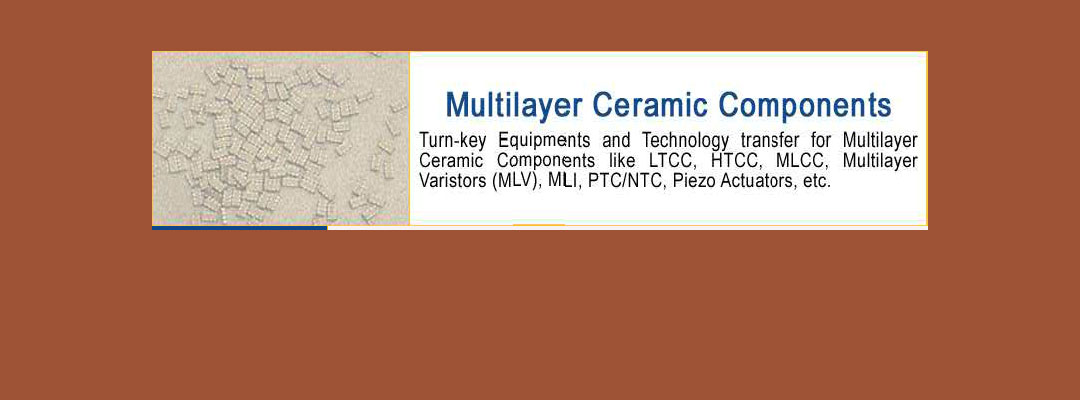
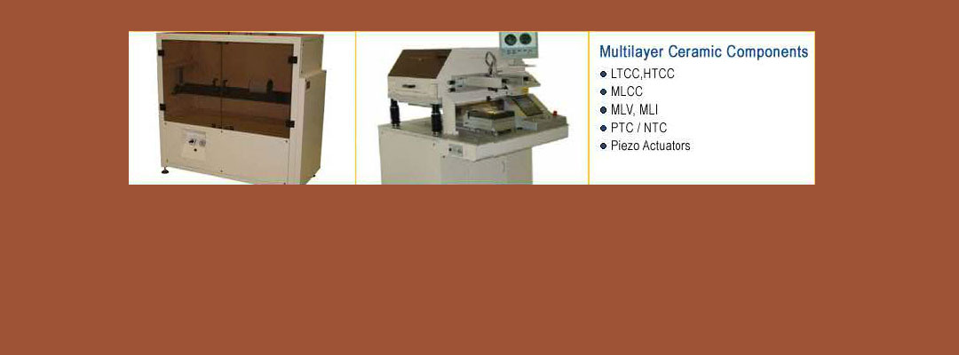
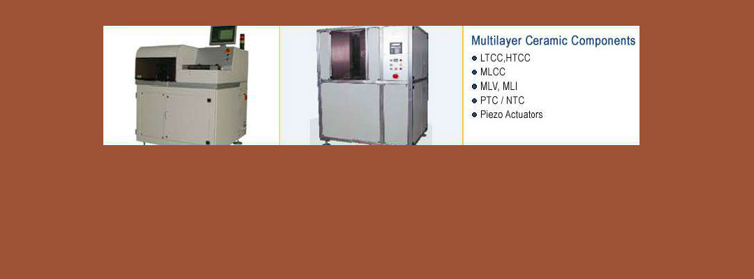
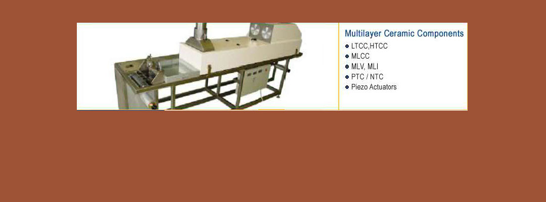
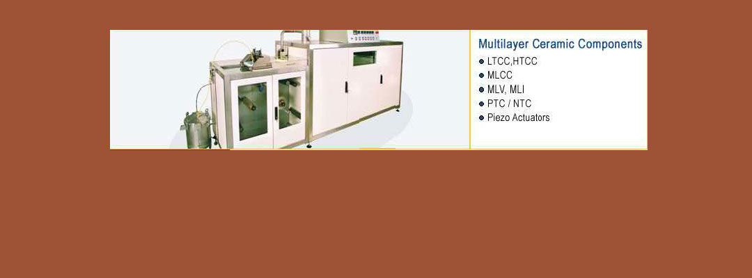
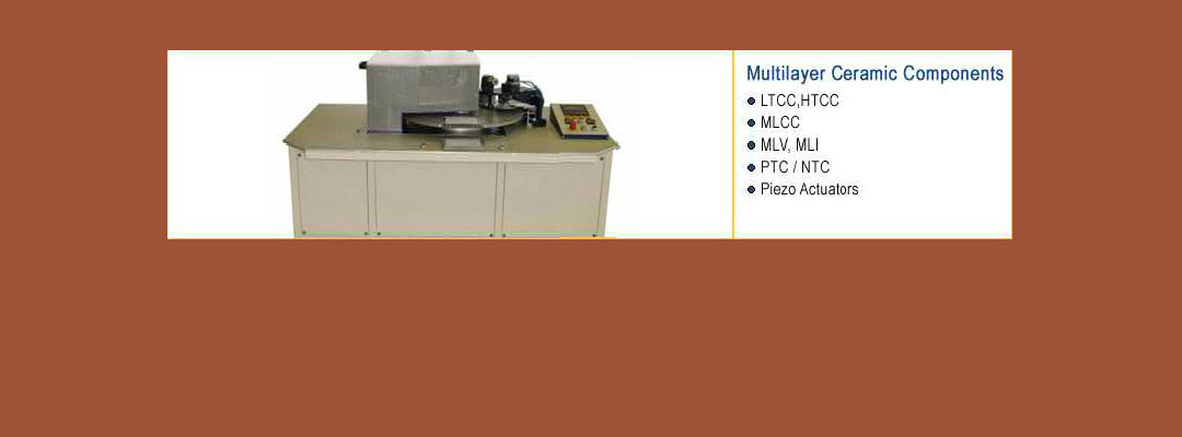
Multilayer Ceramic Components
 Multilayer Ceramic Components sophisticated Telcome and defence or computer systems. The circuits are formed by a thin layer of conducting material deposited, or "printed," on the surface of an insulating board known as the substrate. Individual electronic components are placed on the surface of the substrate and soldered to the interconnecting circuits. Contact fingers along one or more edges of the substrate act as connectors to other PCBs or to other devices such as on-off switches.
There are three major types of printed circuit board construction: single-sided, double-sided, and multi-layered. Single-sided boards have the components on one side of the substrate. When the number of components becomes too much for a single-sided board, a double-sided board may be used. Electrical connections between the circuits on each side are made by drilling holes through the substrate in appropriate locations and plating the inside of the holes with a conducting material. The third type, a multi-layered board, has a substrate made up of layers of printed circuits separated by layers of insulation. The components on the surface connect through plated holes drilled down to the appropriate circuit layer. This greatly simplifies the circuit pattern.
Components on a printed circuit board are electrically connected to the circuits by two different methods: the older "through hole technology" and the newer "surface mount technology." With through hole technology, each component has leads, which are pushed through small holes in the substrate and soldered to connection pads in the circuits on the opposite side. With surface mount technology, stubby J-shaped or L-shaped legs on each component contact the printed circuits directly. A solder paste consisting of glue, flux, and Lead free solder are applied at the point of contact to hold the components in place until the solder is melted, or "reflowed," in an oven to make the final connection. Although surface mount technology requires greater care in the placement of the components, it eliminates the time-consuming drilling process and the space-consuming connection pads inherent with through hole technology.
DIGITAL BULLETINS
Neotronics International LLP is a leading Agency House in the field of PC Board Assembly Line, Semiconductor Packaging, Thick Film and Alternative-Non Conventional Energy. Our close involvement goes right back to the very beginning of this technology.
PRODUCTS
GET US TO CONTACT YOU
(c) 2024 Neotronics International LPP

