Semiconductor Packaging
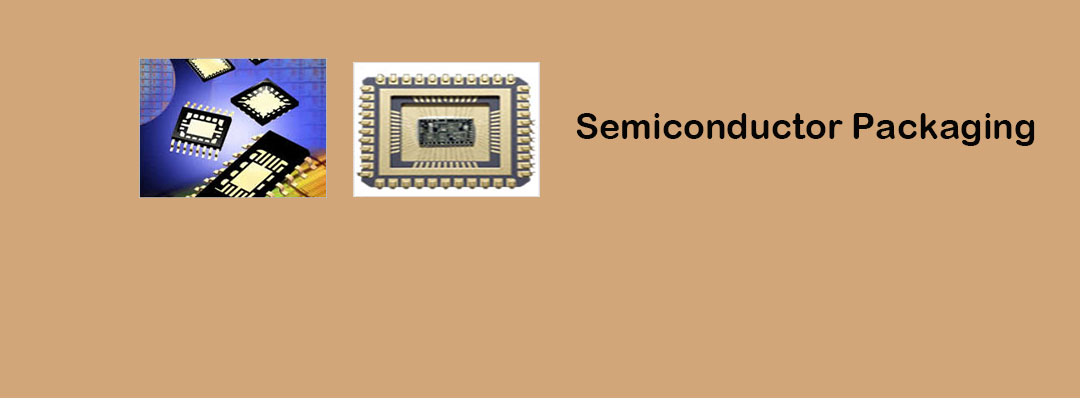
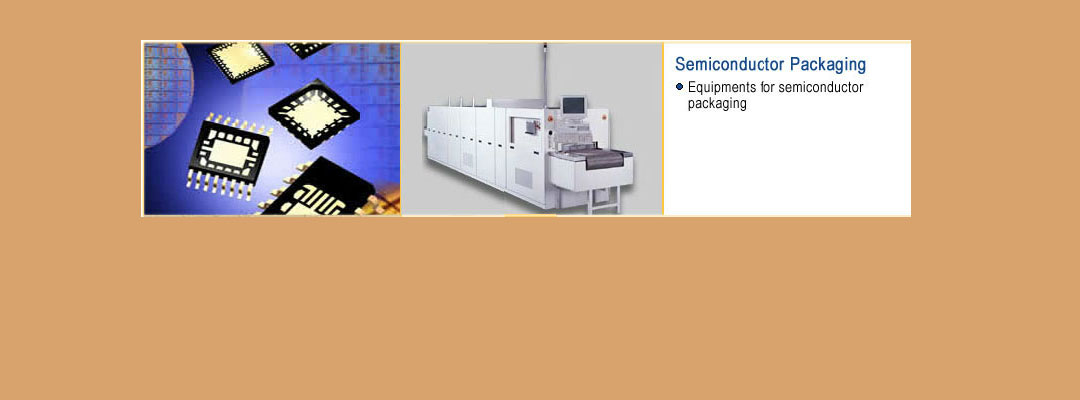
![]() Semiconductor packaging is the process of enclosing of the semiconductor chip or discreet device in the package.
Semiconductor packaging is the process of enclosing of the semiconductor chip or discreet device in the package.
The process flow for semiconductor manufacturing is best considered in two sections, the "front-end" and the "back-end" The "front-end" is wafer processing which is performed in a Wafer Fab area. The process of wafer fabrication is a series of 16-24 loops, each putting down a layer on the device. Each loop comprises some or all of the major steps of photolithography, etch, strip, diffusion, ion implantation, deposition, and chemical mechanical planarization. At each stage, there are various inspections and measurements performed to monitor the process and equipment. Supporting the entire process is a complex infrastructure of materials supply, waste treatment, support, logistics,and automation. It has the cleanest environment in the world.
The "back-end" is Test, Assembly and Packaging, where the finished wafer is split up into individual die (chips) which are then assembled into packages which can be handled in the final applications. Full functional electrical test is performed at both wafer and package level to ensure outgoing quality.Semiconductor Packaging focus on mainstream, back end semiconductor manufacturing processes including: wafer dicing, die bonding, wire bonding, encapsulation, inspection & test, lead forming, sphere attach, singulation and laser marking as well as the materials that constitute the building blocks of semiconductor packages.
Semiconductor Packaging
- Wet Chemical
- Equipments for MEMS
- Wire bonder
- Die bonder
- Wafer Inspection system
- Controlled Atmosphere Furnace
- Flux Coater
- Wafer Loader
- Plasma Ashing system
- Plasma Cleaning System
- Rinser/Dryer Station
DIGITAL BULLETINS
Neotronics International LLP is a leading Agency House in the field of PC Board Assembly Line, Semiconductor Packaging, Thick Film and Alternative-Non Conventional Energy. Our close involvement goes right back to the very beginning of this technology.
PRODUCTS
GET US TO CONTACT YOU
(c) 2024 Neotronics International LPP


